
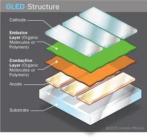
OLEDs are very thin. We are only talking about stacks of material with a thickness of 100–500 nanometers. About 1/200 the size of a human hair. It is a solid-state semiconductor device. Unlike older technologies, it is not dependent on backlight. Instead, the material itself emits light.
Most OLEDs use a two-layer design for their organic components. Some use 3 layers. The additional layers of the three-layer structure only help to transfer electrons from the cathode to the emissive layer. This article focuses on the simpler two-layer architecture. This is the workhorse of most consumer displays.
The Anatomy of an OLED Panel
Building a screen requires precise layering. If the stack is off by a nanometer, the color balance changes or the screen dies. Here is what makes up the final product.
- Substrate : This is the base. You can use clear plastic, glass or thin foil. It provides physical support for everything else.
- Anode : This layer is transparent. It’s all about removing electrons. In physics terms, when an electric current is passed through a device, a “hole” is added to the mixture.
- Organic Layers : These are the active ingredients. They consist of organic molecules or polymers.
- Conducting Layer : This layer moves the “hole” from the anode towards the center. Made from organic plastic molecules. A common polymer used here is polyaniline.
- Emissive Layer : This is where the magic happens. Light is generated here. The conductive layer uses different organic plastic molecules. Transports electrons from the cathode. Polyfluorene is a common polymer for this layer.
- Cathode : This layer injects electrons when the device is powered. Depending on the type of OLED being manufactured, it can be transparent or opaque.
The biggest hurdle in making these screens is the application of these organic layers to the substrate. You cannot just glue them on. This process requires extreme precision. Manufacturers have settled on three main methods to achieve this.
Vacuum Deposition: The Old Guard
The traditional method is called vacuum deposition or vacuum thermal evaporation (VTE). It sounds like a sci-fi procedure, and it is.
The organic molecules are placed in a vacuum chamber. They are gently heated until they evaporate. Then, they are allowed to condense as a very thin film onto a cooled substrate. It’s like making sugar candy, but on an atomic level.
This method works. But it is expensive. This is also inefficient. A lot of material is wasted in the process. For small high-end displays, this may be acceptable. For mass production? Not so much.
Organic Vapor Phase Deposition: A More Efficient Path
Enter Organic Vapor Phase Deposition (OVPD). This method changes the physics slightly to save costs.
OVPD uses a low-pressure, hot-walled reactor chamber instead of pure vacuum. A carrier gas is introduced. The gas transports the vaporized organic molecules to the cooled substrate. Like VTE, the molecules condense into a thin foil.
Why bother using gas? Increase efficiency. Reduce OLED manufacturing costs. By using a carrier, you get better coverage and reduces waste. This is a practical upgrade to the raw thermal evaporation method.
Inkjet Printing: The Future of Large Screens?
The most disruptive method is inkjet printing.
Imagine a standard office printer. Now imagine it spraying liquid light-emitting polymers onto a sheet of plastic. That is essentially what happens here. OLED